

![]()

![]()
Industrial service

The Shanghai Xinsheng Semiconductor Wafer Pulling Plant Phase II Cleanroom and Related MEP Installation Construction Project is located in Pudong New Area, Shanghai. The cleanroom covers an area of...

The Shanghai Ding Tai Jiang Xin 12-inch Automotive Grade Power Semiconductor Automated Wafer Manufacturing Center project aims to build China's first 12-inch automotive-grade power semiconductor wafer fab...

The Shanghai Jita Semiconductor Co., Ltd. Special Process Production Line Construction Project is located in the Heavy Equipment Industrial Zone of Lingang in Pudong New Area, Shanghai. It covers an area of ??230,000...

The Hefei Comprehensive Bonded Zone Electronic Information Standardized Plant Project is part of the development of Crystal Union Integrated Circuit. As the first 12-inch foundry enterprise in Anhui Province...

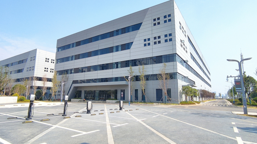
The Shanghai Geke Semiconductor 12-inch CIS Integrated Circuit Feature Process R&D and Industrialization Project is the first large-scale integrated circuit wafer manufacturing project to settle...
The Changsha Anmuquan Advanced Packaging and Testing Expansion Project for High-end Chips is located in the Xiangjiang New Area, Changsha City, Hunan Province, within the Lugu Intelligent Manufacturing Demonstration...
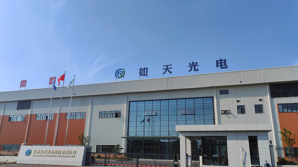
Project Introduction: The Project is located in the High-tech Zone of Rugao City, Jiangsu Province. It is an investment project of Jiangsu Ruting Optoelectronics Technology Co., Ltd. for the production...

Telephone:010-68269396
Address:No. 8, Xiaotun Road, Fengtai District, Beijing

Public account

Video number
Telephone:010-68269396
Address:No. 8, Xiaotun Road, Fengtai District, Beijing
Public account
Video number
